Chemistry
Surface and bulk imaging in blended polymer films

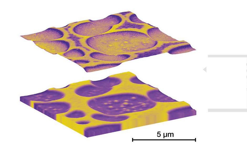
Scanning transmission x-ray microscopy simultaneously generates images of surface and bulk structure.
Cambridge Display Technology Ltd are developing blends of semiconducting polymers to be placed between two electrodes in prototype organic solar cells.
Electrical performance is directly linked to the thin film microstructure and its connection to the electrodes. Common imaging techniques such as atomic force microscopy and electron microscopy lack the chemical sensitivity to decouple surface layer structure and composition from the bulk of the film.
Using instruments at the SLS, phase-separated layered structures of thin films can be uniquely imaged. Scanning transmission x-ray microscopy simultaneously generates images of surface and bulk structure, even for materials with no difference in electron density or constituent atoms. Researchers from the company are studying how polymer droplets with different compositions are found to connect through the layer structure to give good electrical connectivity.
References
Simultaneous surface and bulk imaging of polymer blends with x-ray spectromicroscopy
Watts B, McNeill CR
Macromolecular Rapid Communications. 2010;31:1706.
https://doi.org/10.1002/marc.201000269
