Advanced Materials
Non-destructive 3D x-ray imaging of microchips

Major advance in microchip inspection with x-ray imaging can non-destructively image the 3D design of a microchip.
Electrical wiring and transistors in modern microchips are typically around 30-45 nanometres wide. While it is standard practice to produce structures this delicate, it remains a challenge to measure the exact structure of a finished chip in detail.
Manufacturers mainly use an inspection method in which layer after layer of the chip is removed and then, after each step, the surface is examined with an electron microscope. This is known as focused ion beam/scanning electron microscope imaging (FIB/SEM).
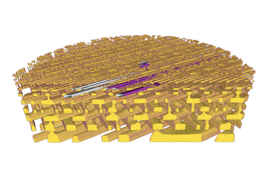
Ptychographic x-ray computed tomography (PXCT) can non-destructively image the 3D design of a microchip with a resolution down to 14.6 nanometres.
The reconstructed three-dimensional images allow the identification of the key parts of the chip, as well as manufacturing artifacts. The technique is also sensitive enough to detect regions of silicon doped with n- or p-type impurities.
The technique offers a major advance in chip inspection and reverse engineering over the destructive traditional methods of electron microscopy and ion milling.
At present, chip pieces of around 10 micrometres can be examined. The method is under constant development, working towards a goal of examining entire microchips within an acceptable measurement time.
References
High-resolution non-destructive three-dimensional imaging of integrated circuits
Holler M, Guizar-Sicairos M, Tsai EHR, Dinapoli R, Müller E, Bunk O, Raabe J, Aeppli G
Nature. 2017; 543: 402–406.
https://doi.org/10.1038/nature21698
